
TSMC projects 4,100 watt chip packages as NVIDIA becomes a data center tenant
Zero One Investment Research Daily Intelligence Brief, September 2, 2026
TSMC projects 4,100 watt chip packages as NVIDIA becomes a data center tenant
Top Market Signals
TSMC moves cooling inside the chip package
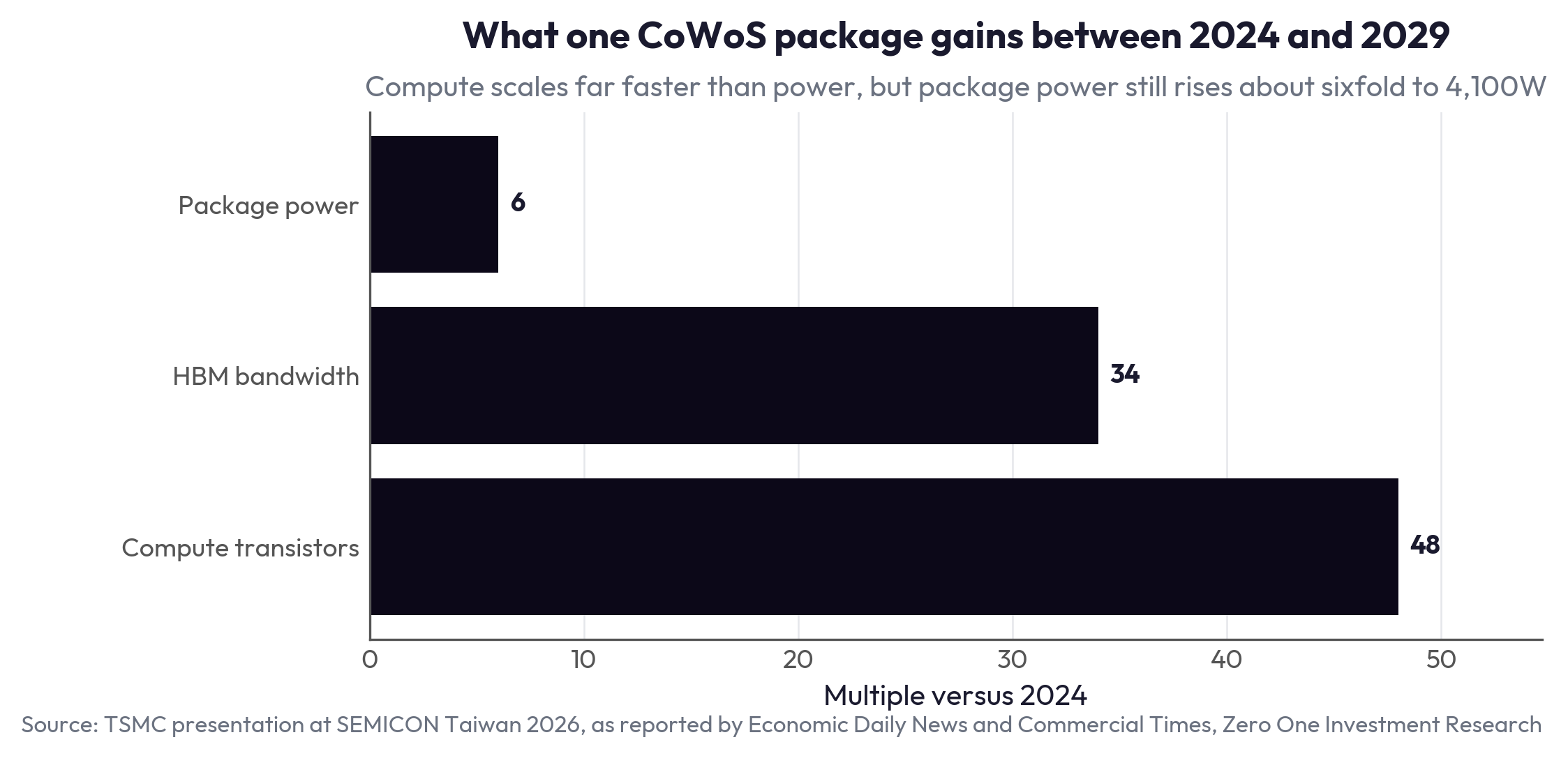
TSMC (2330 TT) confirmed on 1 September that it has added microchannel cooling to its research roadmap, and put a number on why. Chen Yen-ming, who heads advanced packaging research and development, said a single CoWoS (chip-on-wafer-on-substrate) package could draw about 4,100 watts, against roughly 600 watts today, with power delivery losses rising more than fivefold.
Microchannel cooling runs coolant through channels cut into the chip or the package structure itself, so the liquid sits next to the heat source rather than outside it. Today the industry bolts a skived-fin cold plate onto the package lid, and heat still crosses one or two layers of thermal interface material on the way out. The next step integrates the channels into the lid, which cuts that stack from two layers to one. Chen said TSMC is also looking at jet impingement and two-phase boiling.
The scaling math is what forces the change. Between 2024 and 2029, TSMC expects the compute transistors it can fit in one CoWoS package to rise more than 48 times and memory bandwidth more than 34 times, while package power rises about six times. A CoWoS version integrating 24 HBM (high bandwidth memory) stacks across an area larger than 14 reticles is due in 2029. Chen said co-optimizing the lid structure, materials and chip hot-spot layout has already cut junction-to-ambient thermal resistance by up to about 40%.
Taiwan's thermal suppliers are the direct read-across, and the work has moved from the rack to the package. Jentech Precision (3653 TT) already sells a microchannel lid and a vapor chamber lid. I-Chiun Precision (2486 TT) has moved from optoelectronics into chip-level cooling and has sampled package-level parts for NVIDIA's next platform. Auras Technology (3324 TT) says it is sampling now. Industry participants cited by Economic Daily News put microchannel module pricing at three to five times a conventional cold plate, at a higher gross margin. What would change the pace is NVIDIA committing to the technique on a shipping platform rather than a roadmap slide.
Linked stocks: 2330 TT, 3653 TT, 2486 TT, 3324 TT
NVIDIA holds the lease behind Anthropic's US$35bn deal
Anthropic has signed a US$35bn cloud computing contract with Lambda, and the data center that will host it is leased by NVIDIA (NVDA US) itself, according to a Wall Street Journal report. NVIDIA agreed with the developer weeks ago to take the capacity, and Lambda will fill the site with NVIDIA chips it buys.
The building is in Nueces County, Texas, and was built by Hut 8, a bitcoin miner that became a data center developer. NVIDIA is also an investor in Lambda. What Lambda pays NVIDIA for use of the site has not been disclosed.
The arrangement solves two separate problems at once. Anthropic does not carry an investment grade credit rating, which makes long dated compute contracts expensive to underwrite. Lambda, a young cloud provider, did not have to secure a site of its own to win the contract. Anthropic signed a US$45bn agreement earlier this month with Nscale, another NVIDIA-backed cloud provider, for capacity in West Virginia. Hut 8 disclosed in July that a single, very highly rated company had leased its entire 700MW Texas campus for 15 years, a US$20bn facility designed around NVIDIA silicon, without naming the tenant.
Our 31 Aug 2026 Blade covered SB Energy's draft listing document, which said the company's ability to fund an Ohio campus depended on NVIDIA agreeing to a residual value guarantee. Two days later NVIDIA signed for a site rather than guaranteeing one's value. The same pattern runs on the other side of the building: Hut 8 is separately developing a data center for Anthropic that will run Google TPUs, with Google providing financial guarantees so Hut 8 can borrow against it. NVIDIA announced its cloud-provider credit support program in July, and the Wall Street Journal reports it has recently paused some deals under that program, which is the thing to watch rather than the headline contract value.
Linked stocks: NVDA US, 2317 TT, 3231 TT, 2382 TT
Qualcomm raises chip prices as supplier costs climb
Qualcomm (QCOM US) raised chip prices by a double-digit percentage on everything shipped from 1 September, having told customers in July that the new price list was coming. The company said supplier costs have risen far enough that it can no longer absorb them.
Chief executive Cristiano Amon said in a Reuters interview in July that the increase reflects a large rise in supply chain costs and that passing them on was the only option left. That covers the whole price list, not one product line.
The cost is coming from memory. DRAM and storage prices have kept climbing on tight supply, which lifts the bill of materials for every phone and PC. Apple (AAPL US) raised Mac and iPad prices in June, and the iPhone 18 Pro is expected to launch above the price of the outgoing model. Qualcomm's modem chip is still in the iPhone 17 line.
Qualcomm is doing this while its largest single customer shrinks. Amon said in July that revenue from Apple would fall faster than previously expected, by roughly half in the September to December quarter, as Apple moves more of its lineup onto its own C1X modem. Raising list prices into a shrinking Apple book reflects supplier cost pressure rather than Qualcomm's own pricing power. The check is whether handset makers pass it through in 2027 pricing or absorb it in margin.
Linked stocks: QCOM US, AAPL US, MU US, 005930 KS
Samsung Electro-Mechanics books a record MLCC contract
Samsung Electro-Mechanics (009150 KS) disclosed on 1 September a single sales and supply contract for MLCCs (multilayer ceramic capacitors, the passive components that stabilize power delivery on every board) worth KRW1.072tn, about US$778.9m. The company said the order equals 9.5% of its most recent annual revenue.
The contract covers full-year 2027 supply and is the largest long-term agreement the company has signed, according to Korean media cited by DigiTimes. The counterparty is described only as a large global company. AI server demand is the stated driver.
Pricing is moving at the same time. Samsung Electro-Mechanics is expected to raise MLCC supply prices to OEM and ODM customers in 4Q26, with reported increases running as high as 30%, and has already been lifting prices on ABF (Ajinomoto build-up film) substrates. Supply is tight enough that further increases are seen as likely.
MLCCs have historically been sold in short cycles against distributor inventory rather than locked a year ahead, which is what makes one order worth almost a tenth of annual revenue worth noting. A component category that used to be priced every quarter is now being contracted the way memory is. Whether that holds depends on set makers accepting 2027 volumes at prices set before the year begins.
Linked stocks: 009150 KS, 005930 KS, 2327 TT, NVDA US
SK Hynix doubles its wafer spend in one quarter
SK Hynix (000660 KS) roughly doubled what it spent on silicon wafers in 2Q26 against 1Q26, an increase of 104%, while Samsung Electronics (005930 KS) spending on the same input rose only slightly over the period. The company is buying raw material ahead of price increases rather than against current output.
The figure is spend, not volume, and wafer prices are themselves rising, so the two cannot be separated from the reported number alone. What can be read is the direction: one of the two largest memory makers chose to carry the inventory risk and the other did not.
The supplier side describes the same conditions. GlobalWafers (6488 TT) chair Doris Hsu said on 1 September that AI demand is changing what the industry has to supply, that double-digit growth for the silicon wafer sector over the next two years is worth expecting, and that price and volume should rise together.
Buying a commodity input two quarters forward is a position on price direction, taken by a company that can see its own order book. The confirmation to watch is whether Samsung follows in 3Q26, because one buyer stocking up is inventory management and both doing it is a market.
Linked stocks: 000660 KS, 6488 TT, 3436 JT, 005930 KS
China's CXMT begins trial output of AI memory
ChangXin Memory Technologies has started risk production of HBM3E, according to a report by The Information. Risk production is the stage before volume manufacturing, where a process is run on real product to find out what breaks.
CXMT remains a generation behind. Samsung, SK Hynix and Micron are all in volume production on HBM4. Specifications for CXMT's parts are not known, and risk production samples routinely differ from what eventually ships. The JEDEC standard for this generation carries a 1,024-bit interface, transfer rates up to 9.6 GT/s per pin, and 8 or 12 dies per stack, which works out to as much as 1.228 TB/s.
The customers matter more than the specification. Alibaba's T-Head and Cambricon are evaluating the memory with their own processors, and could use it in commercial products as early as next year if qualification runs to plan. Mass production is reported as possible in 2027.
A generation behind is a smaller problem for a buyer who cannot legally purchase the current generation at all. The counterweight arrived the same day: UBS analysts told Bloomberg that China is unlikely to produce a working substitute for ASML's (ASML NA) extreme ultraviolet lithography within the next decade. Memory stacking is a part of the chain China can close with its own capital; the lithography step is not.
Linked stocks: 000660 KS, 005930 KS, MU US, NVDA US
Memory makers move compute into the base die
SK Hynix and Samsung Electronics both spent this week describing the same architectural move, from different stages: putting logic and computation into the base die that sits underneath a memory stack, so that data moves less.
SK Hynix senior vice president Hoshik Kim, speaking at SEMICON Taiwan on 1 September, said a custom HBM design with compute functions in the base die could improve large language model inference performance by up to 5.15 times. His reasoning starts with agentic AI. Multi-turn inference accumulates context, so the KV cache, the stored intermediate state a model reuses between turns, grows exponentially and now matters more than the size of the model's parameters. Moving that data costs thousands to tens of thousands of times the energy of the computation itself.
Samsung set out a three-phase plan at Hot Chips 2026 ending in zHBM, which puts the processor directly beneath the DRAM stack and removes the 2.5D interposer between memory and compute altogether. Sangwook Han of its DRAM design team named the same enabler SK Hynix did: from HBM4, the base die is built on a logic process rather than a DRAM process, in Samsung's case 4nm. HBM4 also doubled data I/O from 1,024 to 2,048 pins, and total stack power keeps rising because bandwidth is scaling faster than energy per bit is improving.
Our 28 Aug 2026 Blade covered NVIDIA doing this from the other direction, with NVHBM moving NVIDIA's own memory controller off the accelerator die and into the base die. The customer went first and both suppliers have now described the same destination. It also puts foundry content inside every memory stack: TSMC said this week that an HBM4 base die on its N12 process cuts power more than 45% and raises bandwidth 2.5 times, with the next generation moving to N3. Kim also described memory becoming a shared data plane across a rack, with the KV cache held once and read by many compute nodes instead of copied between clusters, and said several large data center operators including Alibaba are already building that way. What would settle the economics is whether the memory makers keep the logic base die in house or hand the wafers to a foundry.
Linked stocks: 000660 KS, 005930 KS, 2330 TT, MU US
先聲 First Word: Exclusives from Chinese-Language Sources
TSMC builds a shared advanced packaging validation line in Kaohsiung
TSMC advanced packaging vice president Ho Chun said demand for advanced packaging is growing about 80% a year and should stay strong through 2029, and that TSMC will run a Mini-Loop validation line covering CoWoS process steps at the Baipu park in Kaohsiung. Equipment and materials vendors can put their own labs in the same building, which Ho said cuts adjustment cycles from weeks and months to hours and total validation to under a year. (01 Sep 2026) Source: 台積電進駐高雄白埔園區 先進封裝設備供應鏈再升級
Auras enters NVIDIA's Vera Rubin cold plate chain
Auras Technology (3324 TT) chairman Lin Yu-shen said the company has entered the cold plate supply chain for NVIDIA's Vera Rubin platform and starts shipping in late September or early October, and that full-year revenue growth will now come in above the 70% guided in May. A second Thai plant reaches volume production in September and doubles current capacity, with a third starting construction in 4Q26. (02 Sep 2026) Source: 雙鴻報喜 打入輝達 VR 鏈 最快9月底出貨
JPC Connectivity has 1.6T modules certified at four US customers
JPC Connectivity (6197 TT) chair Chang Shu-mei said order visibility now reaches 2028, and that its 1.6T loop modules have been certified by and are shipping to four US customers. Optical revenue in 1H26 was already double the whole of 2025, and Norway's sovereign wealth fund took a 0.13% stake in the first half. (02 Sep 2026) Source: 佳必琪AI訂單暢旺到後年 1.6T迴路模組出貨美客戶

© 2026 Zero One Investment Research Pte Ltd. For informational purposes only. Not investment advice.